EMI and SI

Reference video
1. How do we Control EMI/SI?
- Contain fields
- Choose ICs with slowest rise/fall times
- Keep high-energy and high-frequency traces as short as possible
- Improve power delivery
2. Signals, Energy, and Fields
- Electric and magnetic fields contain all energy. The energy is not contained in either voltage or current.
- Signal travels in the dielectric space between the conductors.
- copper is a wave guide.
3. Microstrip and Stripline
4. Frequency in the Digital Domain
- Frequency in the digital domain is not clock frequency of MCU or signal
- It is the highest frequency of concern in a system.
- In digital domain we rely on square waves to trnasmit data, but these square waves are not perfect, they has rise and fall time.
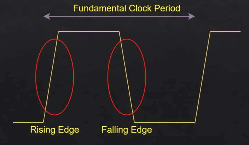
5. Highest Frequency of Concern
Highest frequency content is contained in the rising and falling edges, and this is the maximus frequency that we should be concerned with.
The rising time and falling time are defined by (10% $\rightarrow$ 90%)
-
We can find worst case rising and falling time in IBIS model - Ramp section.
-
The approximation of Highest frequency: $~f_{max,~GHz}\approx\frac{0.5}{t_{~r~~/~f,~ns}}$
This value will affect the trace length when it is comparable to highest frequency.
6. Rise/Fall Times from IBIS Models
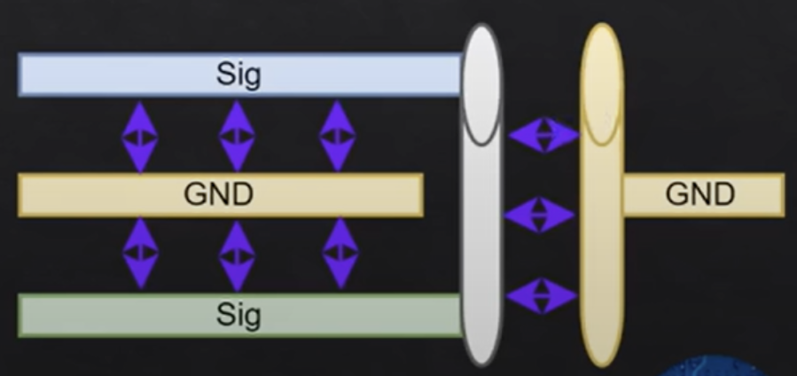
7. Stackup
- Use thin dielectrics between signal and reference plane.
- improve coupling
- reduce inductances
- increase interplanar capacitance
8. Traces and Termination
- Aim to keep as lumped element.
- Traces depends on inner or outer layer routing
- If not lumped, the critical trace length is:
- $ l_{crit}~=~\frac{t_{~r~/~f}~\times~c}{4~~\times~\sqrt{\epsilon}} $
- l in mm, t in ns, c = 300 mm/ns
- outer layer (microstrip) $\epsilon~=~\epsilon_{eff}$
- inner layer (microstrip) $\epsilon~=~\epsilon_{r}$
- Avoid traces near edge of PCB or edge of reference planes
- field will spread out
- Use proper termination
- avoid ringing
9. Vias
- When switching layers, reference (return) switches too. Maintain good return path by placing “transfer via” close to signal via.
- Use microvias, blind or buried vias for better SI $\rightarrow$ reduce stubs
stub: A via stub is the unused part of a via. It does not connect any layers and does not have any any useful function. The unused via or the stub of a multilayer PCBs is the cause for impedance discontinuity in the line.
10. Reference Planes
Solid, unbroken GND plane as reference
-
Do not ever cross a split in a reference plane

Never do this -
Thin dielectrics
- keep reference planes tightly coupled to SIG/PWR layers
- Improve interplanar capacitance
- minimize inductance (decrease loop area)

11. Separation
- X-Y axis separation
- Z axis separation
- Connector placement is an incredibly important part of EMI!