I2C

I2C learning from phil’s lab.

Reference video
I2c Basics
-
multiple devices on a sindle interface
-
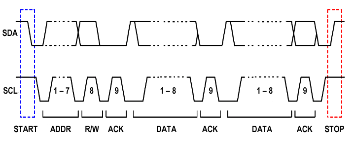
four lines:
- VCC
- GND
- SCL
- SDA
-
three modes of frequencies:
- Standard = 100 kHz
- Fast = 400 kHz
- Fast+ = 1000 kHz
-
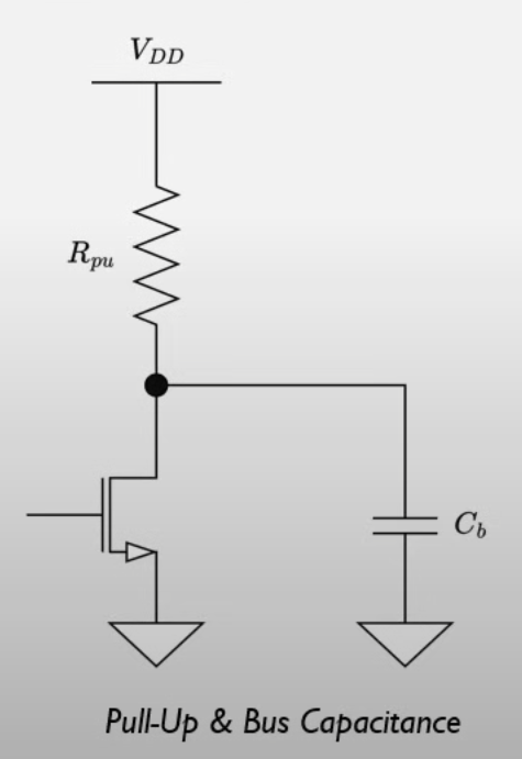
pull-up resistor required to pull to I2C I/O levels (VDD)
- Capacitance on bus (Cb) can’t exceed spec maximum -> related to trace length !!
- rise times is longer than fall times
Capacitance on bus

- Device capacitance: typically, ~10pF for each device (worst case)
- Trace capacitance: 2.2pF per cm (12mil width, 4 mil above reference plant)
- Pad, stray, connector, wire, … capacitance
| Mode | Max. Rise Time (ns) | Max. Capacitance (pF) |
|---|---|---|
| Std | 1000 | 400 |
| Fast | 300 | 400 |
| Fast+ | 120 | 560 |
Pull-up resistors
factors:
- supply voltage +
- power / current consumption +
- interface spped -
- bus capacitance -
$$ R_{pu, min} = \frac{V_{DD, max} - V_{OL, max}}{I_{OL}} $$
where
$V_{DD} =$ I2C leverls voltage
$ V_{OL} =$ low level output voltage
$ I_{OL} =$ low level output current
For example,
Assume $ V_{DD, max} = 3.3 \pm 10% = 3.63V $
From spec we get, $ V_{OL, max} = 0.4V $ and $ I_{OL, max} = 3mA $
$$ R_{pu, min} = \frac{3.63 - 0.4}{0.003} \approx 1.1k \Omega $$
$$ R_{pu, max} = 1.18 \frac{t_{r, max}}{C_{b}} $$
where
$ t_{r, max} =$ maximum rise time allowed
$ C_{b} =$ bus capacitance
For example,
Assume I2C standard mode, $ t_{r, max} = 1000ns $
In the worst case, $ C_{b, max} = 400pF $, $ R_{pu, max} = 1.18 \frac{1000n}{400p} \approx 3.0k \Omega $
Other, if $ C_{b, max} = 50pF $, $ R_{pu, max} = 1.18 \frac{1000n}{50p} \approx 24k \Omega$
Buffer & Level shifters
-
Buffer

- reduce excess capacitance on the bus
- reduce pull-up resistor values while keeping rise times low
-
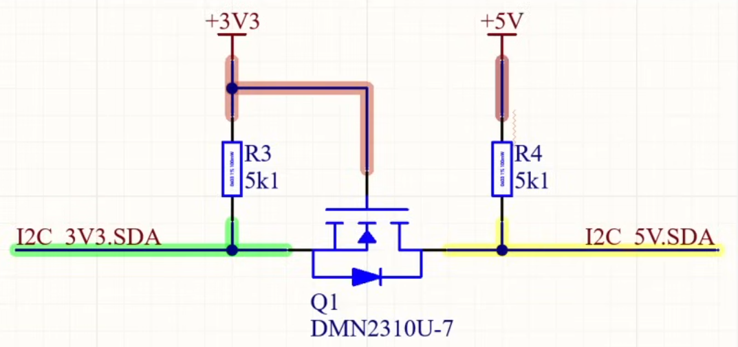
level shifter

- DMN2310U-7 is bidirectional
Layout design advice
- route above reference plane (GND)
- keep the distance between SCL and SCA, and between SCL/SDA and any other … (3 times the dielectric thickness)
- short trace (reduce capacitance)
- put pull-up resistor close to I2C master
- no termination needed

