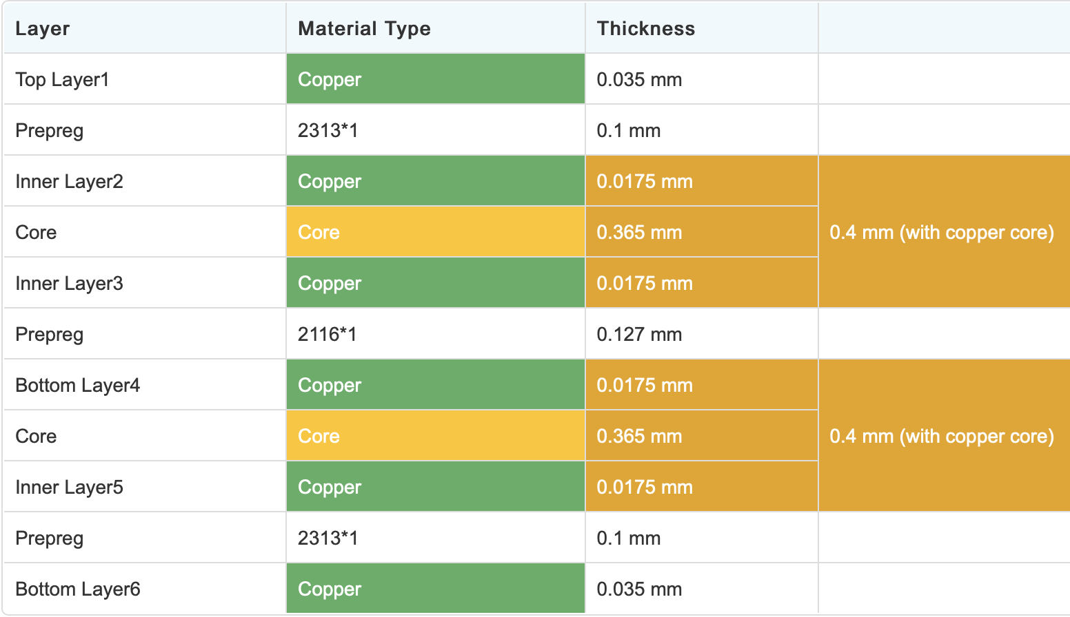
Stack-Up and Build-Up

Contents
Reference video
Build-Up
Build-up explanation
Physical construction of the PCB and its layers
Layer Count
- some constrains
- routing
- density
- package types
- power delivery
- determine overall minumum thickness of PCB
Careful consideration for choosing a stack-up
Dielectric materials
Prepreg
Layer of fiberglass impregnated with resin (e.g. FR-4)
- defined by dielectric constant ($\epsilon_{r}$) and thickness
- type 2116: $\epsilon_{r} = 4.25$
- type 7628: $\epsilon_{r} = 4.6$
Core
Pre-pressed layers consisting of: Copper foil - dielctric - copper foil
- also defined by dielectric constant ($\epsilon_{r}$) and thickness
Copper Foil
- Outer layer
- thicker: 1 oz standard, up to ~ 8 oz
- Inner layer
- thinner: 1 oz maximum, usualy 0.5 oz
Thickness mainly affects current handling capacity
- For exmaple, for an outer layer, 1mm trace (allowed 20 deg temperature rise)
- 0.5 oz: 1.9A
- 1 oz: 3.2A
Manufacturability
-
Manufacturer will calculate for you
-
Example needs
- Desired impedance for target track width
- 0.1 mm track to give 50 ohm SE (single-ended) impedance
- single ended vs differential requirements
TODO: learn what is SE, DE, and how track impedance will affect PCB
Stack-Up
Stack-up is not concerned with the physical/mechanical/material properties of each layer, but rather the electrical properties of each layer in the PCB.
- Determine number of layers
- Assign GND, PWR, SIG layers
TODO: Stack-up pages and references it to here
Layer types
- GND: used as a reference plane/layer for signal traces and power traces/pours.
- PWR: for power distribution, critical for high-speed circuits. Together with GND layers to forms “parallel plate capacitor”. Often various different voltages on a PWR layer.
- SIG: Predominantly trace layers (forward path) using a GND/PWR layer for reference (return path).
Layer assigning goals
- want systematic approach to deciding stack-up
- ensure good EMC/EMI performance
- ensure good signal integrity
- ensure good power delivery
Golden rules
- at AC (above ~kHZ), return path is directly underneath the forward path
- Energy flows in dielectric space between coppers, copper is simply a wave-guide.
- consider both forward and return paths
- want close coupling between SIG + GND, and PWR + GND to prevent fields from spreading (crosstalk and EMI)
- use striplines for higher energy/higher speed signals: GND shield both sides
Power plane
- $C = \frac{~\epsilon_{~r}~\epsilon_{0}~A}{d}$
- bring PWR and GND as close as possible (decrease d):
- increase capacitance
- reduce inductance
Return/transfer vias
WHen we change signal layers with a via, we still need to consider the return path, so we place a GND via cloes to the signal via. Signal energy in via will couple to adjacent GND via.
Additional tips
- Put power layers close to high-speed ICs: minimize via length/inductance for improved power delivery
- Don’t have adjacent SIG layers
- For stack-up with multiple GNDs:
- remember stitching vias
- remember transfer vias
- consider via stubs
- Simple rules: have a minumum one GND reference layer closely to any SIG/PWR
Other factors
- IPC class
- HDI
- backdrills
- controlled impedance
- surface finish